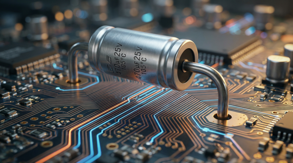
In the world of high-density PCB design, hitting a routing dead-end on a crowded or single-layer board is a common frustration. While most engineers instinctively reach for zero-ohm jumpers, there is a more elegant, dual-purpose solution: the axial electrolytic capacitor. Unlike their radial counterparts, axial capacitors feature long, versatile lead spans that allow them to physically bridge complex traces and leapfrog over congested routing paths.
This “hidden” layout trick provides a mechanical shortcut without sacrificing electrical performance. However, successfully implementing this technique requires more than just creative soldering; you must balance mechanical stability with the risks of accidental short-circuiting while maintaining strict signal integrity. In this guide, we explore how leveraging the unique form factor of axial capacitors can resolve routing bottlenecks, improve power decoupling, and optimize space in layouts where every millimeter counts. Whether you are troubleshooting a legacy board or optimizing a new design, mastering this bridge technique is a vital skill for any hardware engineer.
Understanding the Axial Electrolytic Capacitor: Form Factor vs. Radial Alternatives
While the radial electrolytic capacitor is the industry standard for vertical space efficiency, it fundamentally acts as a “point-of-use” component with a localized footprint. In contrast, the axial form factor—defined by leads extending from opposite ends of the cylindrical body—functions as a strategic topological tool. The primary advantage of the axial capacitor in complex layouts is its span; it effectively serves as a functional bridge, allowing designers to leapfrog over multiple signal or power traces on a single-layer board without the need for vias or zero-ohm jumpers.
In high-density or cost-optimized single-layer designs, routing bottlenecks often occur when a large filter capacitor must be placed near a power rail that is physically separated by signal lines. A radial capacitor would require a circuitous route or a double-sided board to reach both nodes. However, an axial capacitor can be laid horizontally, straddling the intervening traces. This “hidden layout trick” maintains a low center of gravity, which enhances mechanical stability against vibration and shock compared to the high-profile, top-heavy nature of radial alternatives.
From an electrical perspective, designers must account for the slightly higher Equivalent Series Inductance (ESL) inherent in the longer lead spans of axial components. While this makes them less ideal for high-frequency decoupling than surface-mount ceramics, they remain excellent for bulk capacitance and low-frequency ripple filtering. When implementing this bridging technique, it is critical to ensure the capacitor’s heat-shrink insulation is rated for the environment to prevent short-circuiting against the traces it traverses. By treating the axial capacitor as both an energy storage device and a routing bridge, engineers can resolve complex net intersections while maintaining signal integrity and reducing manufacturing complexity.
The Geometry of Advantage: Why Axial Leads Solve Complex PCB Routing Bottlenecks
The fundamental geometric advantage of the axial electrolytic capacitor lies in its ability to serve as a functional “jumper” across a crowded PCB. While radial capacitors are optimized for vertical density, their leads are constrained to a single, tight footprint. In contrast, the axial form factor extends its leads from opposite ends of the cylindrical body, creating a physical span that can leapfrog over multiple signal traces or power rails. On single-layer boards or high-current designs where vias are impractical or cost-prohibitive, this “bridging” capability effectively provides a third dimension of routing on a two-dimensional plane.
From a design perspective, this solves routing bottlenecks by allowing engineers to place bulk decoupling or filtering components directly across congested pathways that would otherwise require complex rerouting. However, successful implementation requires attention to mechanical and electrical nuances. To ensure stability and prevent short circuits when spanning active traces, designers must utilize the capacitor’s outer insulating sleeve as a protective barrier and employ precise lead-forming techniques to maintain air-gap clearance.
While the increased lead length inherent in axial designs can marginally raise Equivalent Series Inductance (ESL) compared to ultra-low ESR radial types, the trade-off is often a cleaner overall layout with fewer inductive loops created by circuitous trace paths. In power decoupling applications, the axial span allows for a more direct connection between a voltage source and a high-draw component, minimizing “necking” in the copper pour. By leveraging the axial capacitor as both an electrical filter and a structural routing asset, designers can resolve layout conflicts that modern surface-mount devices often struggle to navigate in high-voltage or cost-sensitive analog environments.
Bridging the Gap: Using Axial Capacitors as “Component Jumpers” on Crowded Boards
In high-density PCB designs—particularly those limited to single or double layers—the axial electrolytic capacitor serves a dual role: a passive energy reservoir and a strategic “component jumper.” Unlike radial capacitors that occupy a localized footprint, the elongated geometry of an axial unit allows its leads to span several millimeters of board real estate. This enables the designer to leap over congested signal buses or power traces, effectively utilizing the capacitor’s physical body as a bridge that eliminates the need for complex multi-layer vias or zero-ohm jumpers.
Implementing this technique requires a sophisticated approach to mechanical stability and electrical isolation. To prevent short circuits when bridging underlying traces, the capacitor’s aluminum housing must be protected by a high-temperature PVC or polyolefin insulating sleeve. Furthermore, because the component is suspended across a span, it is susceptible to vibration-induced fatigue. Expert designers mitigate this by applying a bead of RTV silicone or non-conductive epoxy between the capacitor body and the PCB, ensuring the solder joints are not the sole point of mechanical failure.
From a signal integrity perspective, the “jumper” approach introduces specific trade-offs. The extended lead length inherent in bridging designs increases Equivalent Series Inductance (ESL). While this is negligible for bulk DC filtering and low-frequency decoupling, it can be detrimental in high-speed switching environments where low-impedance paths are critical. Therefore, axial bridging is most effective for power rail stabilization and audio-frequency coupling. When executed with precision—balancing lead forming for stress relief with strategic placement for thermal dissipation—the axial capacitor becomes a structural asset that resolves routing bottlenecks without compromising the electrical performance of the crowded layout.
Mechanical Stability and Mounting Best Practices for Long-Lead Axial Components
While axial capacitors offer layout flexibility, their horizontal mounting profile introduces unique mechanical challenges that radial counterparts avoid. The primary concern is the “lever arm” effect; the extended lead spans can act as conduits for vibration, potentially leading to fatigue-related failure at the solder fillets or damage to the capacitor’s internal hermetic seal. To ensure long-term reliability, engineers must implement specific mounting protocols.
First, maintain a minimum bend radius for leads—typically at least twice the lead diameter—to prevent micro-fracturing of the wire or excessive stress on the end-cap bung. When bridging complex traces, the capacitor body should ideally be secured to the PCB using a non-corrosive, neutral-cure RTV silicone or specialized mounting clips. This “staking” prevents mechanical resonance and ensures the component remains stationary during thermal cycling or high-shock events.
Furthermore, if the capacitor is utilized as a “jumper” over active traces, electrical isolation is paramount. While the capacitor’s outer sleeve provides nominal insulation, it is not rated as a primary dielectric barrier. Best practices dictate maintaining a “stand-off” clearance or applying high-temperature Kapton tape over the bridged traces to prevent abrasion-induced short circuits over time. From a signal integrity standpoint, keeping the leads as short as the bridging geometry allows minimizes parasitic inductance ($L_{ESL}$), which is critical when the axial component serves as a decoupling element. Finally, ensure that the lead clinching on the solder side is performed in a direction that provides mechanical tension, further anchoring the component against the board surface to prevent “teeter-tottering” during the wave soldering process.
Footprint Management: Integrating Axial Capacitors into KiCad and Modern CAD Workflows
In modern ECAD environments like KiCad, Altium, or Eagle, axial electrolytic capacitors are often relegated to legacy libraries, yet their integration is crucial for executing the “bridge” layout trick. Effective footprint management begins with abandoning static, one-size-fits-all footprints in favor of parametric lead spacing. When defining your footprint in the KiCad Footprint Editor, the lead pitch ($P$) must be calculated as the component body length plus twice the minimum bend radius, plus the specific bridge span required for your routing bottleneck.
To prevent short circuits when the capacitor body spans underlying traces, you must implement specialized Design Rule Check (DRC) strategies. Expert designers should define a “Keep-out Area” on the Top Silk or Courtyard layer directly beneath the component body. This ensures that while the axial leads provide a physical bridge, the CAD engine validates clearance against any underlying high-speed or high-voltage nets. Furthermore, it is vital to account for the component’s height in the Z-axis. Integrating a precise 3D STEP model into your KiCad workflow allows for mechanical collision detection, ensuring the capacitor’s aluminum casing doesn’t interfere with the enclosure or adjacent tall components.
Finally, consider the electrical implications of the extended lead span. In modern CAD workflows, the increased parasitic inductance $(L)$ associated with long axial leads should be noted in the schematic’s design rules. If the axial capacitor is serving a dual purpose—both as a bridge and a power decoupler—ensure the footprint’s loop area is minimized by routing the return path directly beneath the component. By treating the axial capacitor as a strategic mechanical entity rather than a simple passive, you maintain board integrity while bypassing complex multi-layer routing requirements.
Electrical Performance Factors: Analyzing ESR and Dissipation in Axial Form Factors
While the axial form factor is prized for its routing versatility, its electrical performance—specifically Equivalent Series Resistance (ESR) and Equivalent Series Inductance (ESL)—must be carefully quantified to maintain signal integrity. In high-frequency applications, the physical length of axial leads introduces non-negligible parasitic inductance. Unlike radial capacitors, where leads are closely coupled and parallel, the elongated lead path of an axial component increases the loop area, potentially raising ESL by several nanohenries. Designers must account for this shift when the capacitor is utilized for high-speed decoupling or ripple current filtering in switching power supplies.
However, the axial orientation offers a distinct advantage in thermal management and dissipation. The larger surface-area-to-volume ratio of the elongated cylindrical body, often combined with better exposure to lateral airflow across the board, facilitates superior heat dissipation compared to densely packed radial clusters. This is critical when handling high ripple currents that elevate internal temperatures; lower core temperatures directly correlate to a stable Dissipation Factor ($\tan \delta$) and extended component longevity.
Furthermore, when bridging traces, the axial capacitor effectively acts as both a filter and a mechanical jumper. While the ESR is typically comparable to radial equivalents of the same CV (capacitance-voltage) rating, the ESR stability under thermal load is often superior in axial configurations due to reduced thermal crowding. When integrating these into a layout to bypass complex routing, ensure that the proximity to high-impedance traces does not introduce parasitic capacitive coupling or crosstalk. In power-delivery networks (PDN), the axial capacitor serves as a robust bulk reservoir, provided the layout minimizes the trace length from the lead-end to the high-demand load to mitigate the impact of the added lead inductance.
Power Supply Decoupling and Noise Suppression in Single-Layer Layouts
In single-layer PCB designs, the primary challenge is maintaining a low-impedance path for power delivery while navigating dense signal traces without the luxury of internal power planes. This is where the axial electrolytic capacitor serves a dual purpose: it acts as both a high-capacity energy reservoir and a strategic physical bridge. Unlike radial capacitors, which occupy a localized footprint and often require complex “island” routing to reach power rails, the axial form factor allows the designer to span several parallel signal traces to reach the exact VCC or GND node required for effective decoupling.
By bridging across existing copper traces, an axial capacitor can be positioned directly at the pins of an integrated circuit, effectively “jumping” over the routing bottlenecks that would otherwise necessitate zero-ohm resistors or messy jumper wires. This proximity is critical for noise suppression; every millimeter of distance between the capacitor and the IC increases parasitic inductance, which degrades high-frequency decoupling performance. The long axial leads, when kept short and taut, act as low-resistance bus bars, providing a direct path for ripple current and localizing transient spikes before they propagate through the rest of the board.
From a practical implementation standpoint, designers must ensure the component body is properly seated or elevated with insulated sleeving to prevent accidental shorts against the “bridged” traces below. While the extended leads can introduce some parasitic inductance compared to SMD counterparts, the trade-off in a single-layer environment is often a net positive: you gain a cleaner power layout and superior noise suppression by avoiding the tortuous, high-impedance trace paths required by radial components. This makes the axial capacitor an indispensable tool for stabilizing voltage rails in cost-sensitive or space-constrained single-layer layouts.
The Vintage Audio Connection: Why Axial Capacitors are Essential for Restoration and Signal Integrity
In the realm of vintage audio restoration—spanning classic tube amplifiers from Fender and Marshall to high-fidelity Marantz receivers—the axial electrolytic capacitor is not merely a component choice; it is a fundamental requirement for maintaining signal integrity and historical accuracy. Most mid-century audio equipment was engineered using point-to-point wiring, turret boards, or single-sided PCBs designed specifically for the elongated “in-line” lead orientation of axial components.
From a signal integrity perspective, the axial form factor allows for a linear “lead dress” that minimizes parasitic inductance and unwanted coupling. When restoring these circuits, substituting a modern radial capacitor often necessitates “pigtailing” long lead extensions to reach original solder points. This practice is detrimental; these improvised extensions act as small antennas, increasing the circuit’s susceptibility to EMI/RFI and potentially elevating the noise floor with 60Hz hum. Axial capacitors, by contrast, span the original chassis gaps or traces natively, maintaining the designer’s intended current return paths and grounding topology.
Furthermore, the mechanical integration of axial leads provides superior vibration damping in high-gain environments, such as guitar combo amplifiers. The dual-end mounting provides a balanced center of gravity, reducing the risk of lead fatigue or microphonics compared to a top-heavy radial capacitor standing on a single end. For the restoration expert, utilizing high-quality, modern axial capacitors ensures the ESR (Equivalent Series Resistance) remains low enough for ripple current demands while preserving the spatial geometry necessary to prevent crosstalk between sensitive signal stages. Ultimately, the axial capacitor bridges the gap between modern electrical reliability and the preserved sonic character of vintage high-voltage architectures.
Thermal Management and Airflow Considerations for Horizontal Component Placement
When transitioning from radial to axial electrolytic capacitors to solve routing bottlenecks, designers must account for the shift in the board’s thermal profile. Because axial components lay flat against the PCB surface, they occupy a larger horizontal footprint, which can create “airflow shadows.” In forced-convection systems, a large axial capacitor placed perpendicular to the airflow acts as a baffle, potentially starving downstream components—such as voltage regulators or power transistors—of necessary cooling. To mitigate this, orient the capacitor’s longitudinal axis parallel to the primary airflow direction to maintain laminar flow across the board.
Furthermore, the proximity of the capacitor’s cylindrical body to the PCB surface introduces significant thermal coupling. While this can sometimes assist in heat dissipation via the board’s copper planes, it also places the sensitive electrolyte in closer proximity to “hot spots” created by high-current traces or neighboring power resistors. Given that the service life of an electrolytic capacitor is governed by the Arrhenius law—where every 10°C rise in operating temperature can effectively halve the component’s lifespan—strategic spacing is paramount.
When using an axial capacitor as a bridge over existing traces, ensure there is a sufficient air gap or the use of high-temperature insulated sleeving to prevent direct heat transfer from the bridged traces into the capacitor’s casing. This prevents localized heating of the electrolyte and premature ESR (Equivalent Series Resistance) degradation. In high-density environments, prioritizing the placement of axial capacitors in the “cool zones” of the intake, rather than the exhaust side of the enclosure, ensures that your routing solution doesn’t inadvertently become a point of thermal failure.
Safety First: Polarity Documentation and High-Voltage Discharge Protocols
When utilizing axial electrolytic capacitors as functional “bridges” over complex trace networks, safety protocols transition from routine to critical. Unlike their radial counterparts, the physical span of axial leads can obscure the intended polarity orientation during high-density manual assembly. Designers must implement unambiguous silkscreen indicators—specifically a bold “+” or a shaded cathode band—directly adjacent to the respective solder pads to prevent catastrophic dielectric breakdown and subsequent venting. In bridging applications, you must also ensure the capacitor’s insulation sleeve is rated for the potential difference of the traces it traverses to avoid unintended arcing or short-circuiting against underlying copper.
Equally vital is the implementation of high-voltage discharge protocols, particularly in power supply or vintage audio circuits where axial capacitors often reside. Because these components can store significant energy long after the power is removed, engineers should incorporate dedicated bleeder resistors (typically 100kΩ to 1MΩ) into the circuit design to provide a passive discharge path. For maintenance or troubleshooting, manual discharge should never involve a direct short with a screwdriver; instead, use a properly rated discharge tool or a high-wattage resistor to bleed the charge safely. This prevents localized arcing, which can degrade the capacitor’s internal foils or induce transient damage in sensitive low-voltage semiconductors sharing the ground plane.
Finally, always verify a “zero-state” voltage with a calibrated multimeter before making contact with the leads. Designers should be aware of dielectric absorption, where a capacitor seemingly “recharges” itself after discharge, potentially reaching hazardous levels. Documenting these discharge points on the PCB itself is a best-practice methodology for ensuring long-term serviceability and technician safety.
Diagnostic Depth: Using LCR Meters to Evaluate Aging Axial Electrolytic Components
When repurposing an axial electrolytic capacitor as a structural “bridge” across dense PCB traces, the component’s internal health becomes the linchpin of your circuit’s long-term stability. Unlike radial counterparts, aging axial capacitors—particularly those found in vintage gear or legacy industrial controllers—often exhibit electrolyte dehydration that isn’t immediately visible via a standard capacitance meter. To accurately diagnose these components, an LCR meter is indispensable, moving beyond simple microfarad readings to analyze Equivalent Series Resistance (ESR) and Dissipation Factor (DF).
Expert-level diagnostics require setting the LCR meter to the appropriate test frequency; for power-related axial caps, a 100Hz or 120Hz sine wave is standard, while decoupling applications may necessitate 1kHz or 10kHz to reveal high-frequency impedance issues. A rising ESR is the primary indicator of an aging axial component; as the electrolyte diminishes, the ESR climbs, leading to localized I²R heating. This is a critical failure point when the capacitor is horizontally mounted, as it can trap heat against the PCB substrate and accelerate the degradation of neighboring traces.
Furthermore, when using an LCR meter on axial components, the long lead geometry requires specific measurement techniques. Utilizing a 4-wire Kelvin connection is vital to nullify the parasitic resistance and inductance of the leads themselves, ensuring the measurement reflects only the internal chemistry. A high Dissipation Factor (tan δ) often precedes a total loss of capacitance, signaling that the “bridge” is becoming increasingly resistive. For engineers “jumping” critical signal or power traces, ensuring a low DF is non-negotiable to prevent signal attenuation and voltage ripple. By quantifying these metrics, you transform a subjective “re-cap” into a data-driven validation, ensuring your layout trick doesn’t become a latent failure point.
Avoiding Short Circuits: Insulation and Clearance Strategies When Bridging Traces
When utilizing the axial lead of an electrolytic capacitor as a functional jumper to bridge complex traces, the primary design risk is an unintended short circuit caused by lead sag or vibration-induced contact. Because the leads are essentially uninsulated busbars, maintaining rigid clearance and dielectric integrity is paramount.
The first line of defense is the implementation of high-quality heat-shrink tubing—typically polyolefin or PVC—over the span of the lead that crosses over underlying traces. This provides a secondary dielectric barrier, protecting against solder mask abrasions or “pinholing” that can occur over time due to thermal cycling. For high-voltage applications, ensure the sleeve’s dielectric strength exceeds the potential difference between the lead and the traces below.
From a mechanical perspective, the “Z-axis” clearance must be strictly controlled through precision lead forming. Using a dedicated lead-bending tool to create a consistent “bridge” profile—where the lead sits 1.5mm to 3mm above the PCB surface—ensures that the component remains clear of the board’s topography. However, elevation increases the risk of mechanical resonance; therefore, for designs subject to high vibration, “staking” the capacitor body with electronic-grade RTV silicone or a non-conductive epoxy is essential. This prevents the mass of the capacitor from flexing the leads, which could otherwise lead to work-hardening and eventual fatigue failure or parasitic contact.
Furthermore, designers should reference IPC-2221 standards for creepage and clearance distances, especially when bridging high-impedance signal lines or power rails. On the CAD side, implement “keep-out” zones on the top copper layer directly beneath the bridge to mitigate the risk of dielectric breakdown. By combining physical insulation with mechanical fixation and strategic layout constraints, the axial capacitor can safely resolve routing bottlenecks without compromising the long-term reliability of the assembly.
Have questions or your own tips to share? Drop a comment below!